Article written by The Digital Terror
PVD and CVD are both reliable techniques utilized in various industries today.
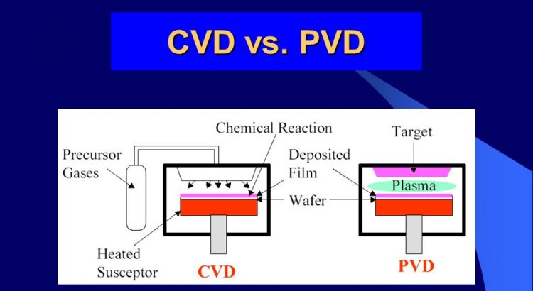
Physical Vapor Deposition (PVD) and Chemical Vapor Deposition (CVD) are two types of deposition techniques that are used to create very thin film layers of a material of choice onto a substrate. Mainly used in the semiconductor production industry, where thin layers are prevalent, both techniques have been making their way into any other industries as well like optics, solar panels, and others. This article will showcase the main differences between the two are the processes that they employ.
As their names imply, PVD utilizes physical forces to deposit while CVD uses chemical reactions. Regardless of the process, both of these techniques produce a thin film in the end.
Physical Vapor Deposition
During the PVD coating process, a source material is gasified through the process of evaporation, the application of electric power, lasers, and other techniques. This evaporated material will then condense onto the substrate, therefore creating the thin film. No chemical reactions occur throughout the process.
Chemical Vapor Deposition
CVD on other hand, uses a source material that is not as pure due to it being mixed with a volatile precursor material. This mixture is then injected within a chamber containing the substrate, where the deposition process occurs, similar to PVD thermal evaporation. Once the mixture adheres to the substrate, the precursor will then decompose, leaving behind a layer of the source material in the substrate. After this, the product is then removed from the chamber through gas flow. This process can also accelerated through the use of plasma, heat, and other processes.